Devices keep getting smaller. Objects that once were only seen with the naked eye now can be looked at through a microscope. How do we keep putting more stuff in less space?
Building technology at the nanoscale, virtually at the atomic level, is the heart of our modern day technological revolution. It seems impossible that engineers can perform such a feat. How do they do it? It turns out some of the techniques used to fabricate at the nanoscale are not as Herculean as one might imagine.
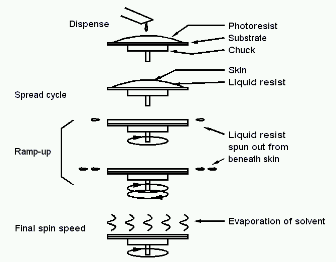
Currently, I work in Dr. Vinod Menon’s Laboratory for Nano and Micro Photonics (LaNMP) at Queens College. The work I do there regularly involves creating structures with very fine thicknesses. For example, I often need to place a layer of material about 400 nm thick on top of a glass piece. The technique I use to accomplish this is called spin coating. There is a device called a spin coater which consists of a rotating platform. I place my glass slide on top of the platform, and use suction to keep it fixed on the mount. I take a liquid solution of my material and place a few drops on top of the glass. The spin coater allows me to adjust the spin speed and spin time. When I let it run, the platform begins to spin rapidly. Because of the centrifugal force caused by the rotation, a lot of the solution flings off the glass slide leaving only a very thin but even layer of material on top of my glass slide that is only nanometers thick. The faster it spins, the thinner it gets. The longer it spins, the thinner it gets.

This week, I went to City College to use one of their devices that allowed me to deposit thin layers of gold on top of a piece of Silicon. The device had an airtight chamber where I placed my samples inside as well as the gold I would be depositing. The gold was held between two metallic fixtures that kept it in place, and the Silicon pieces were laid underneath. The air is sucked out of the chamber to remove any impurities in the process. Because the gold piece is held between two metallic fixtures, I can pass a current through it which would heat up the gold and cause it to vaporize. I raise the current to 50 Amps and the gold piece begins to glow hot. A detector inside displays a reading of how thick the gold layer is and I see that the reading is increasing.
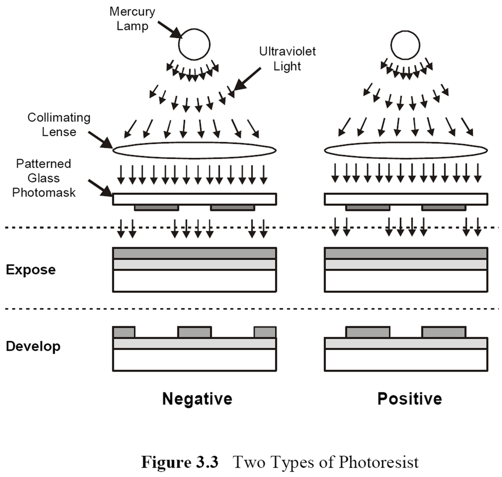
Intel, the largest semiconductor chip making company in the world, also uses special techniques to create their ever increasingly powerful chips. They use a technique called photolithography to fabricate their chips. The way it works is they usually have a base material called a substrate. Then they put a layer of semiconducting material on top of the substrate. This material is sensitive to light, meaning when light is shined on it, it vaporizes. They then put on top of this layer a stencil, that outlines the pattern they want to draw on their chip. Once the stencil is in place, they use light, usually ultraviolet light, to blast away the exposed layers. The parts that are covered by the stencil are kept intact and thus they produce a desired pattern on their chip. They repeat this process with other material as well until they have their completed structure.
There are a number of other techniques that can be used to engineer at the nanoscale. The ones I have mentioned are those that I have been exposed to and had personal experience with. As you can see, building nanoscale structures does not have to involve a very intricate and complicated process. We can use accessible macroscopic techniques to achieve microscopic creations.